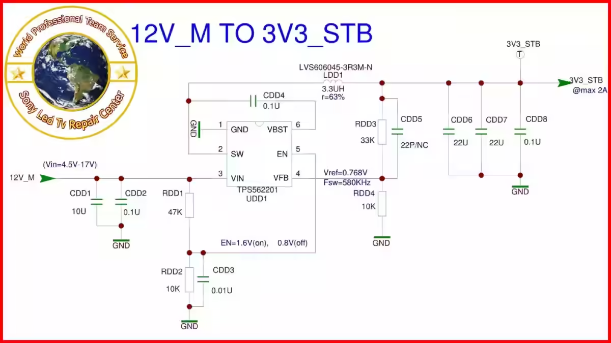
TCL_32S6500_12V to 3V3_STANDBY
schematic diagram. This one is designed to convert a 12V input to a 3V3 output using an IC TPS562201 voltage regulator. The diagram includes various components such as capacitors, resistors, and the vo ltage Regulator itself, each labeled with values and part numbers.

Input (12V)
V_in: The input pin that receives the 12V supply.
Input Capacitor: Typically a capacitor like Cdd1 (10µF/25V) to filter the input voltage and stabilize the power supply.
UDD1 ic {652201}
Pin 1 (GND)
Pin 2 (V_OUT) Switching through coil 3v3
Pin 3 (V_INPUT) 12 voltage in
pin 4 Feedback Resistors: Two resistors forming a voltage divider circuit to provide feedback to the regulator. Common values might be RDD3_33K Link to 3.3V Output and RDD4_10K To GND
Output (3.3V)
pin 5 Enable
3. Output (3.3V)
Output Capacitor: C2 (47µF/6.3V) to smooth the regulated 3.3V output.
sony led tv repair center lahore

im Shuakat Ali
A professional TV technician with 30 yeares of experience
on this website, i share authentic fault finding articles based on my hands-on work
+923214066054
sony.sa.repair@gmail.com
Pingback: TCL_32S6500_12V Input To A 5V - Led Tv Repair Center Lahore
It’s really a cool and helpful piece of information. I’m happy that you shared this useful info with us. Please stay us informed like this. Thank you for sharing.