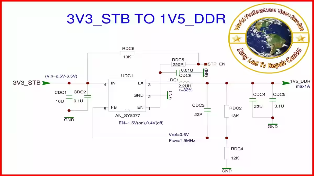
TCL 32S6500 3V3_STB TO 1V5_DDR
schematic diagram for an electronic circuit labeled “3V3_STB TO 1V5_DDR.” This type of diagram is used to represent the connections and layout of an electronic system, including various components like resistors, capacitors, and integrated circuits (ICs).

It seems like you’re asking for information about the transition from 3.3V standby (3V3_STB) to 1.5V DDR (1V5_DDR). Here’s a basic explanation:
In electronics, 3V3_STB refers to a 3.3V standby voltage rail, which is typically used to keep certain circuits powered even when the main device is off. This ensures that essential functions, like memory retention or wake-up signals, remain operational.
On the other hand, 1V5_DDR refers to the 1.5V power supply used for DDR (Double Data Rate) memory, which is a type of RAM commonly used in electronics like TVs or computers.
The transition from 3V3_STB to 1V5_DDR typically involves voltage regulation. A voltage regulator circuit is used to step down the 3.3V standby voltage to the 1.5V required by the DDR memory. This ensures stable and efficient operation of the memory without damaging it by over-voltage.

im Shuakat Ali
A professional TV technician with 30 yeares of experience
on this website, i share authentic fault finding articles based on my hands-on work
+923214066054
sony.sa.repair@gmail.com
Pingback: TCL 32s6500 3.3V STB 1.0V STB - Led Tv Repair Center Lahore
Good sir ji
BHUHOT SHUKRIA SIR
Hello! This post couldn’t be written any better! Reading through this post reminds me of my previous room mate! He always kept chatting about this. I will forward this page to him. Pretty sure he will have a good read. Thanks for sharing!